
기술은 감각이다, 밀론 블로그
[반도체공정 feat.jaeger] 확산(Diffusion) Chapter 4 - 확산 시스템 본문
반응형
반도체 8대 공정 순서
1. 실리콘 웨이퍼 제조 공정
2. 산화공정(Oxidation)
3. 포토공정(Photo)
4. 식각공정(Etching)
5. 증착공정(Deposition)
- 확산(Deposition)
- 이온주입(Ion implantation)
6. 금속배선공정(Metalliztion)
7. EDS 공정(Electrical Die Sorting)
8. 패키지공정(Package)
확산시스템에도 여러 종류가 있습니다.
확산시스템
(1) 밀봉관 시스템 (STS, Sealed Tube System)
(2) 개방관 시스템 (OTS, Open Tube System)
위 두개는 반도체 확산공정에서 가장 많이 사용되는 시스템입니다.

보통 확산공정에서 가격 절감을 위해 여러 장의 wafer 을 한꺼번에 diffusion 합니다.
이렇게 위 사진처럼 여러 장의 wafer 를 동시에 처리하는 것을 batch process 라고 합니다.
(3) 급속 열처리 공정 (RTP, rapid thermal processing)
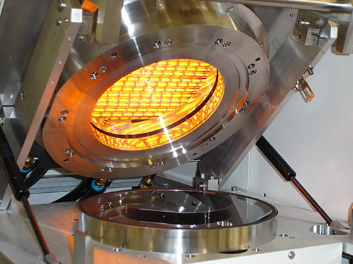
이와 반대로 하나하나의 웨이퍼를 처리하는 것을 single wafer process 라고 합니다.
Halogen lamp 을 사용하여 thermal mass 가 작은 wafer 를 급속 가열을 하여 짧은 시간 확산을 하는 방법입니다.
외부 불순물 침투 최소화, 얕은 깊이의 도핑 가능으로 RTP 공정이 최근에 채택되고 있습니다.
이 공정은 single wafer process 이고 batch process 와 동일한 작업수율을 위해 빠른 공정을 합니다.
이로써 Chapter 4 확산이 끝났습니다.
긴 글 읽어주셔서 감사합니다.
introduction to microelectronic fabrication (Vol 5)
For courses in Theory and Fabrication of Integrated Circuits.The author's goal in writing this text was to present a concise survey of the most up-to-date techniques in the field. It is devoted exclusively to processing, and is highlighted by careful explanations, clear, simple language, and numerous fully-solved example problems. This work assumes a minimal knowledge of integrated circuits and of terminal behavior of electronic components such as resistors, diodes, and MOS and bipolar transistors.
- 저자
- jaeger
- 출판
- 피어슨 에듀케이션
- 출판일
- 2013.08.30
반응형
'반도체 > 확산(diffusion)' 카테고리의 다른 글
'반도체/확산(diffusion)' Related Articles
more


