
기술은 감각이다, 밀론 블로그
[반도체공정 feat.jaeger] 식각(Etch) Chapter 2.3 - dry Etch(건식 식각)이란? 본문
반도체/[공정 4] 식각 공정(etching process)
[반도체공정 feat.jaeger] 식각(Etch) Chapter 2.3 - dry Etch(건식 식각)이란?
milron 2024. 7. 30. 14:00반응형
반도체 8대 공정 순서
1. 실리콘 웨이퍼 제조 공정
2. 산화공정(Oxidation)
3. 포토공정(Photo)
4. 식각공정(Etching)
5. 증착공정(Deposition)
- 확산(Deposition)
- 이온주입(Ion implantation)
6. 금속배선공정(Metalliztion)
7. EDS 공정(Electrical Die Sorting)
8. 패키지공정(Package)
dry etch는 여러 종류가 있습니다.
- 이온빔 스퍼터링 식각(Ion beam spuutering etching)
- RF 스퍼터링 식각(RF sputtering etching)
- 반응건식식각
- 화학적 반응 건식 식각 (chemical dry etching)
하나하나 씩 살펴보겠습니다.
2.2.2. Dry Etch(건식 식각)
건식식각을 하는 이유가 있습니다.
습식식각은 식각이 매우 빠릅니다.
그러나 wet etch는 under cut 현상을 야기합니다.
under cut : 에칭 용액이 깊숙이 침투하여 PR 하부까지 식각 해버리는 현상.
아래와 그림과 같이 under cut 현상을 쉽게 이해할 수 있습니다.
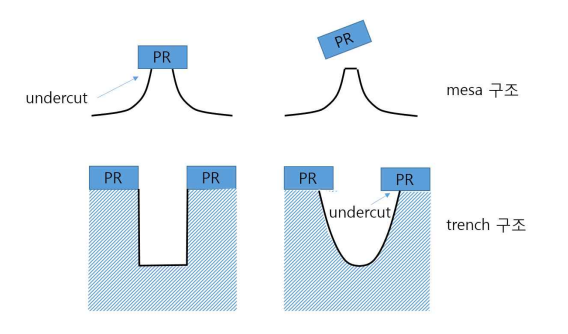
- mesa 구조는 화산처럼 위로 움푹 솟아있는 상태로 wet etching시 하부를 동강 내버립니다.
- trench 구조는 도랑처럼 밑이 파여있어 wet etching시 PR 내부가 깎여나가 원하는 모양으로 다듬기 굉장히 어렵게 됩니다.
dry etch는 wet etch에 비해 폐용액이 적을 수밖에 없기에 상대적으로 환경오염을 덜 시킵니다.
다음은 이온 빔 스퍼터링 식각에 대해 이야기하겠습니다.
감사합니다.
introduction to microelectronic fabrication (Vol 5)
For courses in Theory and Fabrication of Integrated Circuits.The author's goal in writing this text was to present a concise survey of the most up-to-date techniques in the field. It is devoted exclusively to processing, and is highlighted by careful explanations, clear, simple language, and numerous fully-solved example problems. This work assumes a minimal knowledge of integrated circuits and of terminal behavior of electronic components such as resistors, diodes, and MOS and bipolar transistors.
- 저자
- jaeger
- 출판
- 피어슨 에듀케이션
- 출판일
- 2013.08.30
반응형
'반도체 > [공정 4] 식각 공정(etching process)' 카테고리의 다른 글
| [반도체공정 feat.jaeger] 식각(Etch) Chapter 2.3.3 - 반응 건식 식각 장치 (0) | 2024.08.02 |
|---|---|
| [반도체공정 feat.jaeger] 식각(Etch) Chapter 2.3.2 - 반응 건식 식각 (0) | 2024.08.01 |
| [반도체공정 feat.jaeger] 식각(Etch) Chapter 2.3.1- Ion Etch(이온 식각)이란? (1) | 2024.07.31 |
| [반도체공정 feat.jaeger] 식각(Etch) Chapter 2.1 - 식각의 방향은? (0) | 2024.07.29 |
| [반도체공정 feat.jaeger] 식각(Etch) Chapter 2.2 - Wet Etch(습식 식각)이란? (0) | 2024.07.28 |
'반도체/[공정 4] 식각 공정(etching process)' Related Articles
more


